MicroLED Display Technology and Market Outlook
Report Summary
마이크로LED 디스플레이 기술이 비약적으로 발전하며 상용화 초기 단계에 접어들었습니다. 그러나 Apple, 삼성, Facebook 등 기업들의 노력에도 불구하고 신뢰할 수 있는 공급망을 구축과 제조원가 절감이라는 과제가 여전히 남아있습니다. 본 리포트에서는 제조기술의 선택에 따라 달라지는 기술적 과제에 대하여 설명했습니다. 또한 디스플레이 산업의 경쟁 구도에 대한 DSCC의 분석을 바탕으로 2027년까지의 시장 전망치를 담았습니다. 본 리포트는 LED 제조업체와 패널업체, 기술개발자, OEM 업체, 조립 업체, 엔드유저 등 마이크로LED 공급망 내 모든 업체들에게 추천 드립니다.
-
Pages
303 -
File Format
PDF 리포트 -
Order Report
With growing interest in MicroLEDs, DSCC is proud to announce a new report on MicroLED Display Technology and Market Outlook.
MicroLEDs have garnered a lot of interest because of the potential advantages over other flat-panel display technologies, most notably in high efficiency, high brightness, high color saturation, faster response rate, and longer lifetime. This unique combination of features would make MicroLED the superior display for many applications, ranging from super large TVs to microdisplays for use in AR/VR headsets. The ability to withstand harsh environmental conditions is also particularly attractive for the automotive industry.
MicroLEDs have generated a lot of hype, but also a lot of confusion amongst the mainstream media. This is because MicroLED displays can be manufactured in different ways, and each one will bring its own set of challenges and possible applications.
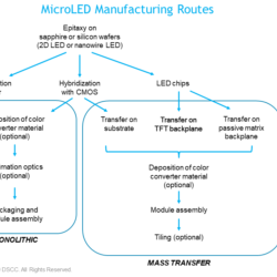
The report covers the two general manufacturing methods: monolithic or mass transfer. The monolithic approach is the preferred route to make microdisplays that are below 1-inch in diagonal and with a very high pixel density above 5,000 PPI. These miniature displays are very promising for AR/VR since they can achieve millions of nits in brightness without sacrificing contrast or compactness. However, obtaining a full color display has proven to be a challenge.
The mass transfer approach consists in moving a large number of individual MicroLEDs on the display substrate. This method can, in theory, produce displays of any size, including large TVs above 100-inch in diagonal. There are currently several mass transfer technologies under development.
Samsung has already started selling luxury MicroLED video walls to consumers. However, the LED chips on these displays are still larger than 100 μm, which is the commonly accepted size definition for a MicroLED. Future MicroLED TVs will be based on smaller LED chips, which will help reduce the total BoM of the display. However, shrinking the LED chips too much can have an impact on efficiency and affect the performance of the display.
The report covers all these issues in detail and shows the various solutions under development by the MicroLED industry. The report also includes market forecasts to 2027, segmented by applications.
TABLE OF CONTENTS
1. Introduction and Executive Summary p. 5
- Recent Announcements
- Market Forecast Summary
- Overview of MicroLED Applications
- MicroLED Manufacturing Routes
- Current Status of MicroLED TVs
- MicroLED Displays for AR/VR
2. MicroLED Supply Chain p.23
- Samsung
- Apple
- Meta
- Snap
- Vuzix
- Xiaomi
- TCL
- Konka
- Sony
- Ennostar
- PlayNitride
- AUO
- Foxconn
- Seoul Viosys
- Ams OSRAM
- Aledia
- VueReal
- Jade Bird Display
- MICLEDI Microdisplays
- Plessey Semiconductors
- Mojo Vision
- Nanosys
3. Epitaxy & Chip Manufacturing p.63
- Epitaxy by MOCVD
- 2D vs. 3D MicroLEDs (Nanowires)
- Sapphire vs. Silicon Substrates
- Chip Structure
4. MicroLED Efficiency p.88
- External Quantum Efficiency (EQE)
- Why Efficiency is a Challenge
- Improving MicroLED Performance
5. Monolithic MicroLED Displays p.104
- Monolithic Displays
- Various Approaches to Hybridization
- Sapphire vs. Silicon Wafers
- CMOS Backplane
- Wafer Mismatch
- Micro-optics
- Challenges with Colors
- Combining Displays
- QD Color Conversion
- Native Colors
- Porotech
6. Mass Transfer Processes p.133
- Overview of Mass Transfer Processes
- Stamp Based
- Laser-Assisted
- Fluidic Assembly
- Continuous/Semi-continuous
- Other Techniques
7. Yield & Defect Management p.180
- Yield Management with Mass Transfer
- Redundancy
- Test and Repair
- Defect Management and Compensation
- Defects in Monolithic Displays
8. Color Conversion p.199
- Quantum Dot Color Conversion (QDCC)
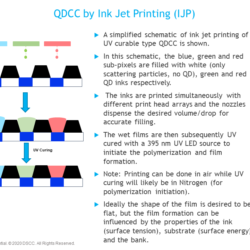
- Photolithography Vs Inkjet Printing
- Key Optical Properties for QDCC: Blue Absorption, External Quantum Efficiency, Color Gamut
- Key Players and Demos
- Phosphors
9. Display Driving and Backplane p.225
- Challenges of Driving MicroLEDs
- Passive Matrix
- Active Matrix TFT Backplanes
- Microdriver IC
- Smart Pixels
10. Additional Functionalities for MicroLED p.243
- Transparent Display
- Flexible Display
- Embedded Sensors
11. MicroLED Cost Analysis p.253
- Epiwafer Consumption
- Backplane Cost
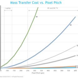
- Mass Transfer Cost
- Color Converter Cost
- Cost Reduction Strategies
12. MicroLED Market Analysis and Forecasts p.270
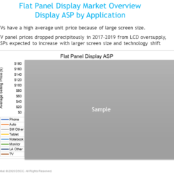
- Flat Panel Display Market Overview
- Competitive Landscape
- Shipment and Revenue Forecasts (2022 to 2027)
Report Samples
제품 카탈로그 다운로드
DSCC는 매년 100건 이상의 디스플레이 산업 관련 리포트를 발간하고 있습니다. 우리의 사명은 모든 디스플레이 기반 제품에 대한 worldwide/end-to-end 서플라이체인에 대한 종합적인 분석을 제공하는 것입니다.